


Semiconductor Inspection System Market Introduction
The semiconductor inspection system market plays a critical role in maintaining the performance, reliability, and yield of semiconductor devices throughout the manufacturing process. These systems are used to detect defects and ensure quality control at various stages of semiconductor fabrication, including wafer, mask, and packaging inspection. As the complexity of integrated circuits increases, driven by miniaturization and the demand for higher performance chips, inspection systems become indispensable for defect management and process optimization.
The rapid advancement of semiconductor technologies—such as 3D stacking, FinFET, and extreme ultraviolet (EUV) lithography—has led to heightened demand for more sophisticated and precise inspection tools. In this context, semiconductor inspection systems not only aid in early fault detection but also contribute to reducing production costs by minimizing yield losses. Additionally, with the growing global reliance on electronics and digital infrastructure, the need for highly efficient and accurate semiconductor production has become even more crucial.
The market is further bolstered by rising investments in semiconductor fabrication plants, particularly in regions focusing on technological self-sufficiency. Increasing demand across various end-use sectors such as consumer electronics, automotive, healthcare, and industrial applications contributes significantly to the expansion of the inspection system market. Moreover, the growing integration of AI and machine learning in inspection technologies is paving the way for real-time defect analysis and intelligent manufacturing.
Overall, the semiconductor inspection system market is expected to experience sustained growth due to technological innovations, expanding semiconductor demand, and the ongoing push for enhanced manufacturing quality. The market dynamics will be shaped by both macroeconomic trends and advancements in semiconductor device architecture, making it a vital area of interest for stakeholders throughout the semiconductor value chain.
Semiconductor Inspection System Market Definition
A semiconductor inspection system refers to an advanced technological solution used during the fabrication of semiconductors to identify and classify physical and functional defects. These systems utilize a range of optical, electron beam, and X-ray-based techniques to examine wafers, photomasks, reticles, and packaged chips for imperfections that could compromise device performance. The primary objective is to detect defects early in the process to avoid yield loss and ensure high product reliability.
There are two main types of inspection: optical and electron beam-based. Optical inspection systems are typically used for rapid, large-area defect detection, while electron beam systems offer higher resolution for detecting extremely small defects in advanced nodes. Inspection can be conducted at various stages of production, including front-end (wafer) and back-end (packaging) processes. Key functionalities of these systems include pattern inspection, surface inspection, and critical dimension (CD) metrology.
Semiconductor inspection systems have evolved significantly with technological advancements. Traditional manual inspections have been replaced by automated systems that can scan and process high-resolution images in real-time. These tools are essential in controlling process variability and achieving the stringent quality requirements demanded by modern applications.
In addition to defect identification, inspection systems play a crucial role in data analytics. The insights gathered from inspection processes help in root cause analysis, yield enhancement, and continuous improvement of manufacturing operations. They also contribute to the development of more reliable and robust semiconductor devices by ensuring that only components meeting quality standards progress to the next stage of production.
In essence, semiconductor inspection systems act as the gatekeepers of quality in the semiconductor industry. Their accuracy, speed, and integration with production lines are fundamental to enabling high-throughput and defect-free manufacturing in today’s competitive semiconductor landscape.
Semiconductor Inspection System Market Scope & Overview
The scope of the semiconductor inspection system market encompasses the entire semiconductor manufacturing ecosystem, from design and prototyping to full-scale production and packaging. These systems are integral to maintaining yield, minimizing defects, and ensuring high-quality production at every stage of the value chain. The market spans across various inspection types including wafer inspection, mask inspection, and packaging inspection, offering diverse opportunities for technological advancement and business expansion.
The global market has gained traction due to the increasing need for high-performance chips used in consumer electronics, automotive electronics, telecommunications, data centers, and industrial automation. As the industry progresses toward smaller process nodes (e.g., 5nm and below), the demand for more advanced inspection systems capable of detecting minute defects has intensified. Innovations in artificial intelligence, deep learning, and real-time analytics are further expanding the capabilities of these systems.
Additionally, as integrated circuit designs become more complex, with features like 3D chip stacking and multi-chip modules, inspection systems must evolve to accommodate these changes. Their ability to handle new geometries, materials, and layers is vital for ensuring manufacturing integrity and reducing failure rates.
The market also covers a variety of system types, including in-line and off-line inspection systems, with integration into smart manufacturing environments becoming increasingly prevalent. This convergence with Industry 4.0 technologies is allowing manufacturers to automate quality control processes and implement predictive maintenance strategies.
Overall, the semiconductor inspection system market offers robust potential for innovation and investment. With the growing proliferation of electronics across all sectors, coupled with rising demand for data processing and connectivity, the importance of maintaining high-yield semiconductor production will continue to drive the market’s growth. The scope is global and multi-dimensional, making it an essential pillar of the semiconductor manufacturing ecosystem.
Semiconductor Inspection System Market Size
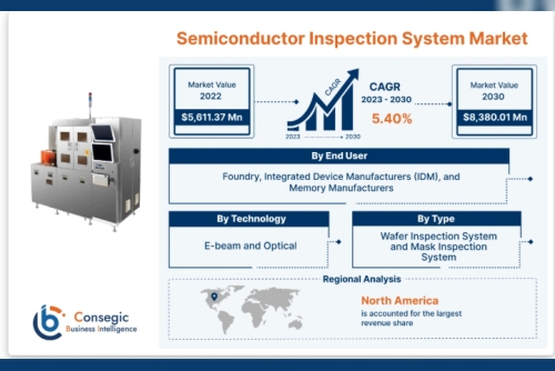
Semiconductor Inspection System Market size is estimated to reach over USD 8,380.01 Million by 2030 from a value of USD 5,611.37 Million in 2022, growing at a CAGR of 5.40% from 2023 to 2030.
Semiconductor Inspection System Market Segmental Analysis
The semiconductor inspection system market can be segmented based on product type, technology, end-use application, and inspection stage.
By Type
Wafer Inspection System and Mask Inspection System
By Technology
E-beam and Optical
By End User
Foundry, Integrated Device Manufacturers (IDM), and Memory Manufacturers
Semiconductor Inspection System Market Key Industry Drivers & Trends
The semiconductor inspection system market is driven by several key industry forces and emerging trends. One of the primary drivers is the miniaturization of semiconductor devices. As manufacturers transition to smaller nodes, such as 7nm, 5nm, and beyond, the detection of increasingly minute defects becomes critical, necessitating more advanced inspection tools.
Another significant driver is the growing complexity of semiconductor architectures. The emergence of 3D ICs, chiplets, and multi-die packages requires more intricate inspection solutions capable of analyzing multiple layers and interfaces. As chip designs become more compact and multifunctional, inspection systems must evolve in precision and adaptability.
The demand for high-yield and high-reliability chips, especially for automotive and mission-critical applications, further fuels the need for advanced inspection. Automotive semiconductors, in particular, require rigorous testing due to their deployment in safety and performance-critical systems.
Artificial intelligence and machine learning are also transforming the market. These technologies enhance defect classification, enable predictive analytics, and reduce false positives, thereby increasing manufacturing efficiency. AI-powered systems are becoming standard in modern fabs for real-time decision-making and automated quality control.
Another trend shaping the industry is the integration of inspection systems into smart factories. With the rise of Industry 4.0, semiconductor manufacturers are adopting connected, intelligent equipment that supports remote monitoring, data analytics, and system optimization.
Geopolitical factors and supply chain shifts are also influencing market dynamics. As regions strive for semiconductor self-sufficiency, investments in new fabs are creating additional demand for inspection systems.
In summary, miniaturization, advanced packaging, smart manufacturing, and the push for higher yield and efficiency are driving trends in the semiconductor inspection system market. These factors are expected to continually reshape the technological landscape and spur long-term market growth.
Semiconductor Inspection System Market Regional Analysis
The semiconductor inspection system market exhibits strong geographical diversity, with key regions including North America, Asia-Pacific, Europe, Latin America, and the Middle East & Africa. Each region plays a distinctive role in the global semiconductor ecosystem and contributes uniquely to market growth.
Asia-Pacific is the dominant region in the semiconductor inspection system market, largely due to the presence of major semiconductor foundries and extensive manufacturing infrastructure. Countries such as South Korea, Taiwan, China, and Japan are central to global chip production and are investing heavily in inspection technologies to enhance yield and competitiveness. The growing demand for consumer electronics, coupled with governmental incentives for semiconductor independence, fuels robust regional expansion.
North America holds a significant market share, driven by advanced research facilities, a strong presence of integrated device manufacturers, and high adoption of leading-edge technologies. The region is also a hub for innovations in AI and advanced inspection systems. Investments in new fabrication plants and a focus on domestic semiconductor production are boosting demand for inspection solutions.
Europe is another important region, particularly in terms of industrial automation and automotive semiconductor applications. The region's push toward technological sovereignty and investment in high-tech manufacturing is expected to support market growth. European nations are also actively participating in collaborative semiconductor projects and research initiatives.
Latin America and the Middle East & Africa are emerging markets with potential for future growth. As global semiconductor consumption rises and localized production begins to gain attention, these regions may present new opportunities for inspection system deployment.
Overall, regional growth is influenced by the maturity of semiconductor manufacturing ecosystems, government policies, and levels of investment in R&D and infrastructure. As global demand surges, cross-regional collaborations and supply chain realignments will continue to shape the future of the semiconductor inspection system market.
Semiconductor Inspection System Market Key Players
ViSCO Technologies USA, Inc., TAKANO CO., LTD., UENO SEIKI CO., LTD., Nikon Metrology NV., Toray Engineering (TASMIT, Inc.), Onto Innovation, Inc., C&D Semiconductor Services Inc., Lasertec Corporation, KLA Corporation, Applied Materials Inc., Hitachi Group, ASML Holding N.V., and JEOL Ltd.
Contact Us:
Consegic Business intelligence
Email : [email protected]
Sales : [email protected]