


3D Semiconductor Packaging Market
Introduction
The 3D semiconductor packaging market is rapidly emerging as a critical segment within the broader semiconductor industry, driven by the growing demand for high-performance, compact, and energy-efficient electronic devices. Unlike traditional 2D packaging, 3D packaging leverages vertical stacking of chips—often interconnected through through-silicon vias (TSVs)—to deliver enhanced functionality, faster data transfer, and reduced power consumption. This innovative approach is becoming essential in enabling next-generation technologies such as artificial intelligence (AI), machine learning (ML), Internet of Things (IoT), 5G, and autonomous vehicles.
As electronic devices become more sophisticated and miniaturization trends continue, manufacturers are turning to 3D packaging to overcome the limitations of Moore’s Law and traditional scaling. Key applications include mobile devices, data centers, automotive electronics, consumer electronics, and high-performance computing. Furthermore, ongoing R&D investments and strategic collaborations among key industry players are fostering innovation in advanced packaging materials and design architectures.
3D Semiconductor Packaging Market Size
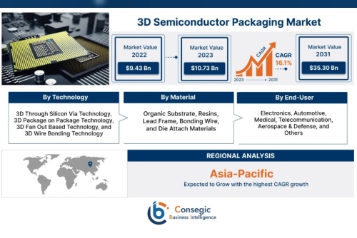
3D Semiconductor Packaging Market size is estimated to reach over USD 35.30 Billion by 2031 from a value of USD 9.43 Billion in 2022 and is projected to grow by USD 10.73 Billion in 2023, growing at a CAGR of 16.1% from 2023 to 2031.
3D Semiconductor Packaging Market Scope & Overview
The scope of the 3D semiconductor packaging market encompasses the comprehensive study of advanced packaging technologies that enable the vertical stacking of integrated circuits (ICs) to enhance performance, reduce form factor, and improve energy efficiency. This market includes various 3D packaging approaches such as Through-Silicon Via (TSV), 3D System-in-Package (3D SiP), 3D Integrated Circuits (3D ICs), and Fan-Out Wafer Level Packaging (FOWLP). These technologies are increasingly adopted in diverse applications including smartphones, high-performance computing, data centers, automotive electronics, and consumer devices.
This report provides an in-depth analysis of the market from 2023 to 2031, covering key factors such as market size, growth drivers, technological innovations, application segments, and regional dynamics. It explores both the current landscape and future outlook, highlighting trends such as the shift toward heterogeneous integration, chiplet-based designs, and the increasing relevance of advanced interconnect solutions.
3D Semiconductor Packaging Market Dynamics (DRO)
Drivers:
Increasing Demand for Miniaturized and High-Performance DevicesAs consumer electronics become more compact and powerful, there is a growing need for advanced packaging solutions that offer higher performance within smaller footprints. 3D packaging enables stacking of ICs, which optimizes space while improving speed and power efficiency. Rapid Adoption of AI, IoT, and 5G Technologies
The evolution of AI, IoT, and 5G networks is accelerating the demand for advanced semiconductor solutions. 3D packaging plays a critical role in meeting the performance and bandwidth requirements of these applications by enabling high-density interconnects and improved thermal management. Growing Complexity in Chip Designs
As Moore’s Law slows, chipmakers are turning to heterogeneous integration and chiplet architectures, both of which rely heavily on advanced 3D packaging technologies to interconnect different components in a single package efficiently. Rise in Data-Centric Applications
The explosion of data from applications like cloud computing, autonomous vehicles, and edge devices has heightened the demand for faster, more efficient chips—fueling growth in the 3D packaging sector.
Restraints:
High Initial Cost and Complex Manufacturing Process3D semiconductor packaging involves advanced equipment, skilled labor, and costly materials, which can increase production costs and limit adoption, especially for smaller manufacturers. Thermal Management Challenges
While stacking chips improves performance, it also poses thermal dissipation issues. Managing heat in densely packed 3D architectures remains a key technological challenge. Limited Standardization
The lack of standardization in 3D packaging technologies can lead to integration issues and limit interoperability, particularly when combining chiplets from different vendors.
Opportunities:
Expansion in Automotive Electronics and EVsThe rising adoption of electric vehicles and advanced driver-assistance systems (ADAS) opens up vast opportunities for 3D semiconductor packaging, especially in power management and sensor integration. Growth of Edge Computing and Data Centers
As more computing power shifts to the edge and data centers expand, there is a significant opportunity for 3D packaging solutions that offer low latency and high-speed processing. Advancements in Packaging Materials and AI-Driven Design
Innovations in materials science, combined with AI-enabled chip design tools, are expected to streamline the 3D packaging process and reduce costs over time. Government and Industry Support for Semiconductor Supply Chains
Strategic investments and policy incentives in regions like the U.S., China, South Korea, and the EU are promoting the development of local semiconductor ecosystems, which in turn benefit the 3D packaging sector.
3D Semiconductor Packaging Market Segmental Analysis
By Technology:
Through-Silicon Via (TSV) Offers high interconnect density and performance Widely used in high-performance computing and memory applications 3D Integrated Circuits (3D ICs) Vertically integrated chips with active interconnects Used in advanced microprocessors and GPUs 3D System-in-Package (3D SiP) Combines multiple components in a single package Common in mobile and consumer electronics Fan-Out Wafer-Level Packaging (FOWLP) Cost-effective alternative with improved thermal performance Increasingly used in smartphones and wearable devices Others Including 2.5D packaging and hybrid bonding techniquesBy Material:
Organic Substrates Widely used due to low cost and flexibility Leadframe Traditional packaging material, still used in some legacy systems Ceramic Offers excellent thermal performance; used in military and aerospace Silicon Interposer Critical for 2.5D/3D ICs and high-speed data processing Die Attach Materials (Solder Paste, Adhesives, Films) Enable bonding and thermal conduction in 3D stacked designs Encapsulation and Underfill Materials Provide structural support and protection for 3D assembliesBy End-User Industry:
Consumer Electronics Smartphones, tablets, AR/VR devices, and wearables Automotive Advanced Driver Assistance Systems (ADAS), EVs, and infotainment systems Telecommunication 5G infrastructure, base stations, and network equipment Healthcare Medical imaging, diagnostics, and wearable health monitors Industrial Automation, robotics, and sensor networks IT & Data Centers High-performance computing, memory modules, and AI acceleratorsBy Region:
Asia-Pacific Dominates the market with strong manufacturing hubs (China, Taiwan, South Korea, Japan) Rising demand from consumer electronics and automotive industries North America Driven by technological innovation, especially in AI and data centers (U.S. and Canada) Europe Growth driven by automotive and industrial automation sectors Latin America Emerging market with increasing investment in electronics and telecom infrastructure Middle East & Africa Gradual adoption fueled by smart city initiatives and digital transformation
Top Key Players & Market Share Insights
The 3D semiconductor packaging market is highly competitive and characterized by the presence of several global and regional players. Market leaders are continuously investing in R&D, strategic collaborations, and capacity expansion to strengthen their market position. These companies play a crucial role in advancing 3D packaging technologies and shaping the industry landscape.
Top Key Players:
Amkor Technology ASE Technology Holding Co. Ltd Siliconware Precision Industries Co. Ltd JCET Group Intel Corporation Taiwan Semiconductor Manufacturing Company Limited (TSMC) Sony Corporation Samsung Electronics Co., Ltd. 3M Company Advanced Micro Devices Inc. (AMD)
Contact Us:
Consegic Business intelligence
Email : [email protected]
Sales : [email protected]