


Semiconductor Inspection System Market
Introduction
The semiconductor inspection system market plays a crucial role in ensuring the quality and reliability of semiconductor devices. As semiconductor manufacturing processes become increasingly complex and miniaturized, the demand for advanced inspection technologies has surged. These systems are essential for detecting defects, contamination, and process variations at various stages of chip fabrication, thereby minimizing production errors and improving yield. With the rapid growth of industries such as consumer electronics, automotive, and telecommunications, the semiconductor inspection system market is witnessing significant innovation and expansion globally.
Semiconductor Inspection System Market Size
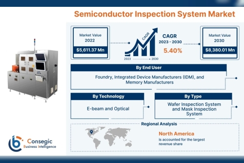
Semiconductor Inspection System Market size is estimated to reach over USD 8,380.01 Million by 2030 from a value of USD 5,611.37 Million in 2022, growing at a CAGR of 5.40% from 2023 to 2030.
Semiconductor Inspection System Market Scope & Overview
The semiconductor inspection system market encompasses a wide range of technologies and solutions designed to identify defects and irregularities in semiconductor wafers and chips during the manufacturing process. This market includes inspection tools such as optical inspection systems, electron beam inspection, and X-ray inspection, each catering to different stages of semiconductor fabrication. The scope extends across various applications, including front-end wafer inspection, back-end packaging inspection, and final testing. Growing demand for smaller, faster, and more efficient semiconductor devices drives the need for high-precision inspection systems. Additionally, advancements in AI and machine learning are increasingly integrated into inspection technologies, enhancing defect detection accuracy and process control. The market serves diverse end-users from semiconductor foundries, fabless companies, and integrated device manufacturers, contributing to the overall growth and innovation in the semiconductor industry.
Semiconductor Inspection System Market Dynamics (DRO)
Drivers:
Increasing complexity and miniaturization of semiconductor devices requiring advanced defect detection. Growing demand for high-quality, reliable semiconductor products in electronics, automotive, and telecommunications sectors. Rising adoption of automation and AI-driven inspection systems for improved accuracy and efficiency.Restraints:
High initial cost and maintenance expenses associated with advanced inspection equipment. Technical challenges in detecting nanoscale defects as semiconductor nodes shrink. Limited availability of skilled workforce to operate and maintain sophisticated inspection systems.Opportunities:
Expansion of semiconductor manufacturing in emerging markets creating new demand. Integration of machine learning and big data analytics to enhance defect prediction and process optimization. Increasing focus on quality control in next-generation semiconductor technologies like 5G, IoT, and AI chips.
Semiconductor Inspection System Market Segmental Analysis
By Type:
Inline Inspection Systems: Used during wafer fabrication for real-time defect detection. Offline Inspection Systems: Conduct detailed analysis outside the production line to identify defects.By Technology:
Optical Inspection: Utilizes light-based methods to detect surface and pattern defects. Electron Beam Inspection: Employs electron beams for high-resolution defect detection at nanoscale. X-ray Inspection: Uses X-rays to inspect internal structures and packaging defects. Other Technologies: Includes advanced methods like atomic force microscopy and infrared inspection.By End-User:
Semiconductor Foundries: Use inspection systems to ensure high yield and quality in mass production. Integrated Device Manufacturers (IDMs): Employ inspection tools for in-house chip fabrication and testing. Fabless Companies: Rely on third-party inspection services for quality assurance.By Region:
North America: Leading region with advanced semiconductor manufacturing and inspection tech adoption. Asia-Pacific: Fastest-growing market driven by expanding semiconductor fabs in China, Taiwan, and South Korea. Europe: Focuses on innovation and high-precision inspection systems for niche semiconductor segments. Rest of the World: Emerging markets showing gradual growth in semiconductor inspection demand.
Top Key Players & Market Share Insights
ViSCO Technologies USA, Inc. TAKANO CO., LTD. UENO SEIKI CO., LTD. Nikon Metrology NV. Toray Engineering (TASMIT, Inc.) Onto Innovation, Inc. C&D Semiconductor Services Inc. Lasertec Corporation KLA Corporation Applied Materials Inc. Hitachi Group ASML Holding N.V. JEOL Ltd.
Contact Us:
Consegic Business intelligence
Email : [email protected]
Sales : [email protected]